
The inventors of the transistor and the integrated circuit received Nobel Prizes. The engineering community marks anniversaries of their conception with conferences, banquets, and awards. Occasionally they are even celebrated in the popular media.
So why has no one heard of the inventor of the diode? After all, in the form of the solar cell and the increasing popular LED (light emitting diode) lamp, to the average consumer it is probably the most visible product of the semiconductor electronics revolution that The Atlantic magazine recently hailed as the fourth most important invention since the wheel.
One reason could be that it was discovered nearly 150 years ago; in the same era as the telephone (Atlantic #24). Another is the complex lineage of its evolution. The popular media prefers a simple story with a single hero. Literally hundreds of engineers and scientists have made important contributions to the success of the diode.
My interest in the history of the diode was stimulated by my review of the Fairchild Semiconductor patent notebooks early this year. This revealed a substantial effort into the development of a wide variety of new diode products that continued well into the 1970s, even after integrated circuits had emerged as the industry’s primary driver. Some of the researchers and types investigated included Grinich (four-layer diodes), Noyce (negative resistance diodes), Saxena (hot electron diodes), Wilson (Schottky diodes), Kromer, who did receive a Nobel Prize (Gunn effect diodes), Allison (Zener diodes), and Last and Wheeler (light emitting and light sensing diodes).
This blog outlines the people and stories behind this humble but surprisingly sophisticated device that continues to play an important role in computing, communications, and consumer electronics.
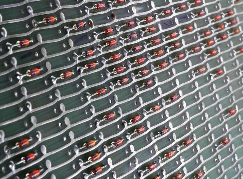
Diode matrix board for a PDP-11 floppy disk boot Read Only Memory (circa 1970). Each bit in the ROM is represented by the presence or absence of a diode. Courtesy: Dave Fischer, Providence, Rhode Island
A diode is a two-terminal electronic device that allows current to flow easily in one direction while presenting a high resistance in the reverse direction. Diodes have performed a wide variety of functions in computers. In 1950, the National Bureau of Standards Eastern Automatic Computer (SEAC) employed 10,500 germanium diodes as the first machine to use semiconductor devices as logic switches. In succeeding machines they also served in roles as diverse as memory storage elements and high-voltage power supply rectifiers. Light emitting and sensing properties continue to enable displays and input/output devices for fiber-optic interconnections.
William Shockley’s single-minded pursuit of a novel four-layer diode device he conceived as a replacement for electro-mechanical relays in telephone switching systems played an important role in the history of Silicon Valley. Realizing that his idea was ahead of its time, in 1957 eight of his key employees quit Shockley Semiconductor Laboratory in Mountain View in frustration to start Fairchild Semiconductor where they focused on improving silicon transistors.
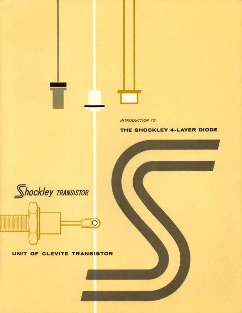
Brochure cover for Shockley 4-Layer Diode. Circa 1960.
Originally called a rectifier because of its ability to convert alternating current (AC) to direct current (DC), it was renamed a diode in 1919 by English physicist William Henry Eccles who coined the term from the Greek root di, meaning “two”, and ode, a shortened form of “electrode.” The latter was itself coined by scientist Michael Faraday from the Greek words elektron (meaning amber, from which the word electricity is derived) and hodos; way, path, road, or connection.
The complexity of this etymology is entirely appropriate. While the physical structure of a diode may appear deceptively simple, in addition to rectification, light emission, light sensing, and negative resistance characteristics, semiconductor diodes extend their capabilities into every conceivable electrical and electronic system from radar microwave detectors to the widely used light emitting diode (LED) lamp. The two fundamental diode structures, thermionic (vacuum tube) and solid state (semiconductor), were discovered within 12 months of each other in the second half of the 19th century.
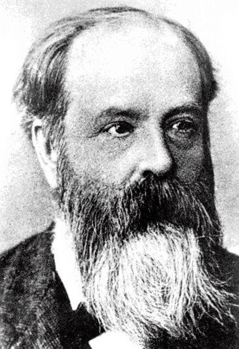
Frederick Guthrie (1833–1886) discovered the thermionic diode in 1873
In 1873, English scientist Frederick Guthrie noted that placing a white-hot metal plate connected to ground close to, but not actually touching, a positively-charged electroscope would discharge the instrument. This did not happen when the electroscope carried a negative charge.
In 1880, William J. Hammer, assistant to Thomas Edison at his Menlo Park, New Jersey laboratory, reported a blue glow around the positive pole and a blackening of the wire at the negative pole of an early electric light bulb. Originally called “Hammer’s Phantom Shadow,” his employer renamed the phenomenon the “Edison Effect,” when he patented the incandescent light bulb in 1883.
Both researchers had independently discovered the heat-induced flow of charge in one direction known as thermionic emission but neither envisaged any practical application for their work. Twenty years later, former Edison employee John Ambrose Fleming realized that the effect could be used as a detector for radio signals. Fleming patented the thermionic diode, the first practical vacuum tube electronic device, in Britain in 1904.
German physicist Ferdinand Braun, a 24-year old graduate of the University of Berlin, studied the characteristics of electrolytes and crystals that conduct electricity at Würzburg University. In 1874 while probing galena crystals (lead sulfide) with the point of a thin metal wire, he noted that current flowed freely in one direction only. Braun had discovered the electrical rectification effect that takes place at the point of contact between metals and certain crystal materials. Braun demonstrated this semiconductor device at Leipzig in 1876, but it found no useful application until the advent of radio in the early 1900s.
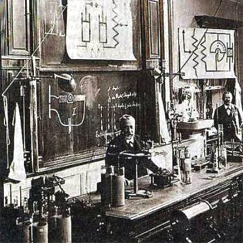
Ferdinand Braun (1850 –1918) discovered the semiconductor diode in 1874
C.E Fitts constructed a current rectifier using selenium in the U.S. circa 1886. His work did not result in any practical devices until it was revived in the 1930s where it found wide application as an efficient means of converting AC voltage to DC in industrial applications with relatively large power requirements.
In 1901, Jagadis Chandra Bose, a professor of physics in Calcutta, India, filed a U.S patent for a galena crystal point-contact semiconductor diode for detecting radio signals. Beginning in 1902, American Telephone and Telegraph engineer Greenleaf W. Pickard tested thousands of mineral samples to assess their rectification properties. He filed a patent for a silicon point-contact detector in 1906 and subsequently founded the Wireless Specialty Apparatus Company to market “cat’s whisker” crystal radio detectors. His was probably the first company to make and sell commercial silicon semiconductor devices. Many other inventors experimented with alternative materials. Henry Dunwoody received a patent for a carborundum (silicon carbide) detector just two weeks after Pickard. Wichi Torikata earned a Japanese patent for a mineral detector in 1908.
Although semiconductor devices allowed simple radio sets to operate without external power, by the mid-1920s the more predictable performance of vacuum tube diodes replaced them in most radio applications. Semiconductors regained prominence in World War II as radar detectors because of their ability to operate at microwave frequencies.
The arena of light emitting diodes has been particularly rich in pioneering work. In a letter to Electrical World in 1907, H. J. Round, an English radio pioneer working for Guglielmo Marconi in New York, described electroluminescence from a crystal of carborundum (silicon carbide). This is the first known report of light emission from a semiconductor, the principle behind the modern LED lamp.
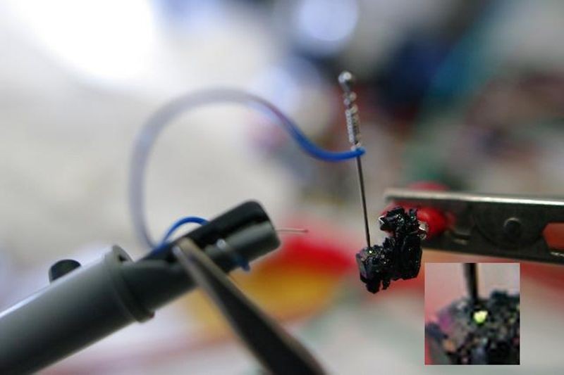
Replication of H. R. Round’s demonstration of light emission (inset) from Silicon Carbide Courtesy: Biolippi (2009)
In 1922-23, Russian engineer Oleg Losev reported light emission from a radio crystal and in 1927 filed a patent for a ‘light relay’ that proposed his devices “for fast telegraphic and telephone communication.” This work foreshadowed the development of optoelectronic diodes that are fundamental to modern fiber optic links.
Rubin Braunstein of the Radio Corporation of America reported infrared emission from gallium arsenide (GaAs) in 1955. Two researchers at Texas Instruments, James R. Biard and Gary Pittman, were awarded the first LED patent, and Nick Holonyak Jr. of the General Electric Company has been called “the father of the LED” for developing the first practical device that emitted in the visible spectrum in 1962.
Translated into English as “semiconductor,” the German word “halbleiter” was first used in 1911 to describe materials with electrical conductivities between those of metals (conductors) and insulators. But an explanation of semiconductor behavior eluded scientists for decades. As late as 1931, physicist Wolfgang Pauli opined that “one shouldn’t work on semiconductors, that is a filthy mess; who knows whether any semiconductors exist.”
Satisfactory explanations of rectification in a semiconductor device finally emerged in 1938. Boris Davydov at the Ioffe Physico-Technical Institute of the Russian Academy of Sciences, Leningrad, Nevill Mott at Bristol University, England, and Walter Schottky at Siemens and Halske in Munich, Germany independently attributed the phenomenon to a concentration of electrons on the semiconductor surface that set up an asymmetric barrier to current flow.
While investigating the use of silicon diodes as radar detectors in 1940, Russell Ohl, an electrochemist at Bell Telephone Labs in Holmdel, NJ, tested a small silicon slab that yielded strange results. When exposed to bright light, the current flowing through the slab jumped appreciably.
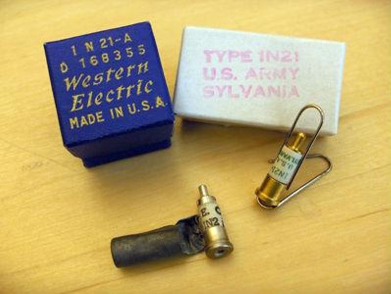
Typical examples of WWII microwave frequency crystal rectifiers in the museum collection
Ohl and colleague Jack Scaff found that a seam in the slab marked the separation of the silicon into regions containing distinct kinds of impurities. One impurity, the element phosphorus, yielded a slight excess of electrons in the sample while the other, boron, led to a slight deficiency (later recognized as “holes”). They called the regions n-type (for negative) and p-type (positive); the surface or “barrier” where these regions met became known as a p-n junction. Light striking this junction stimulated electrons to flow from the n-side to the p-side, resulting in an electric current. Ohl had discovered the photovoltaic effect that powers today’s solar cells.
The work of Ohl and Scaff led to a giant leap forward in semiconductor material technology as silicon and germanium diodes were deployed for the war effort. Researchers in Great Britain and the United States developed techniques to purify both elements and “dope” them with selected impurities to obtain the desired characteristics. Countless microwave frequency diodes were fabricated for use in Allied radar receivers. Semiconductor material quality improvements flowing from this work enabled the fabrication of the first transistor at Bell Labs in 1947.
Semiconductor diodes and transistors gradually replaced vacuum tubes in digital computers during the 1950s. By 1960, all new designs employed semiconductors for logic functions. The wide range of other possible applications that had emerged for the diode since its discovery stimulated research in labs worldwide into how new manufacturing techniques could be applied to produce better devices for electronic systems. When combined with Jean Hoerni’s revolutionary planar process, the work described by the researchers at Fairchild yielded new commercial products that contributed important sources of revenue in the early days of the company.
With this long history involving hundreds of engineers and scientists across the world, is it appropriate to anoint any one of them as “the inventor of the diode?” Some would bestow the honor on those who first discovered the effect (Guthrie and Braun). Others support the candidacy of those who patented the first useful devices (Fleming and Bose). Etymologists may vote for those who coined the name (Eccles and Faraday). My preference is to recognize that this is one of so many examples in the history of science and technology where success has many fathers, including in this case those early researchers at Fairchild Semiconductor.