
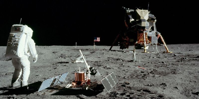
Buzz Aldrin at work on the Moon, July 20, 1969. Photo: NASA
In his speech before a joint session of Congress on May 25, 1961, President John F. Kennedy also noted that “in a very real sense, it will not be one man going to the Moon —if we make this judgment affirmatively, it will be an entire nation. For all of us must work to put him there.”
Even as the president was speaking, engineers at Fairchild Semiconductor, a hot new tech startup in Mountain View, California, were putting the finishing touches to the electronic industry's first family of microelectronic integrated circuits (ICs). Meanwhile, at the Massachusetts Institute of Technology Instrumentation Laboratory (MIT/IL) in Cambridge, Massachusetts, a team was preparing a proposal to NASA that would employ those circuits, popularly known today as “computer chips,” in a computer (the Apollo Guidance Computer—AGC) small and powerful enough to guide that man safely to the Moon and back.
This is the story of these people, deeply involved in “work to put him there,” and how a decision to employ this unproven technology, criticized at the time as reckless, helped to launch the integrated circuit as an essential building block of today's digital world.
Researchers across Europe and the United States pursued the use of semiconductor materials to control the flow of electric current as an alternative to bulky, power-hungry vacuum tubes for much of the first half of the last century. Scientists at Bell Telephone Laboratories in New Jersey demonstrated the transistor, the first device to serve that need, in 1947. As the transistor's advantages of small size, low power, and improved reliability became widely understood, early uses in hearing aids and portable radios quickly expanded into computers, instruments, and avionics systems.
Guidance controls for Cold War−era missiles presented an important early application. Charles Stark Draper, founder of MIT's Instrumentation Laboratory, pioneered inertial navigation techniques that allowed aircraft to locate their position by continuously sensing changes in direction and speed. When physicist Eldon C. Hall, originally destined for a career as a farmer in Oregon (a background that Nobel Prize−winning laser inventor Charles Townes claims trains a person “to solve practical problems and fix things innovatively”) joined the lab in 1952, he was assigned the task of developing a digital upgrade for current analog systems to meet demands for increased accuracy.¹ In 1956, Hall completed the design of a germanium transistor-based digital system for inertial navigation of the Navy's Polaris submarine-launched missile. Transistors for this program were built on a dedicated production line by Texas Instruments (TI).
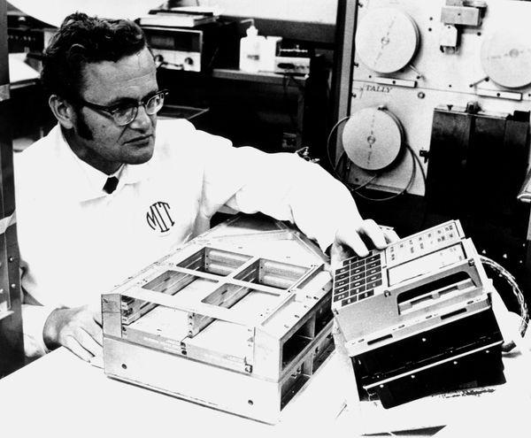
Eldon Hall inspects an AGC display and keyboard (DSKY). Photo: Charles Stark Draper Laboratory Archives
In March 1959, TI announced engineer Jack Kilby's success in building a “solid-circuit” using all semiconductor components to reduce the size and weight of airborne equipment. Using microscopic gold wires, Kilby connected a transistor, a capacitor and two resistors fashioned from a slice of transistor material into an electronic oscillator circuit. Researchers at Bell Labs, IBM, RCA and other laboratories had already demonstrated all semiconductor circuits, but they served only specialized needs with few applications. Kilby's approach offered a more general-purpose solution to miniaturizing electronic systems and enjoyed enthusiastic management support for its commercial promise.
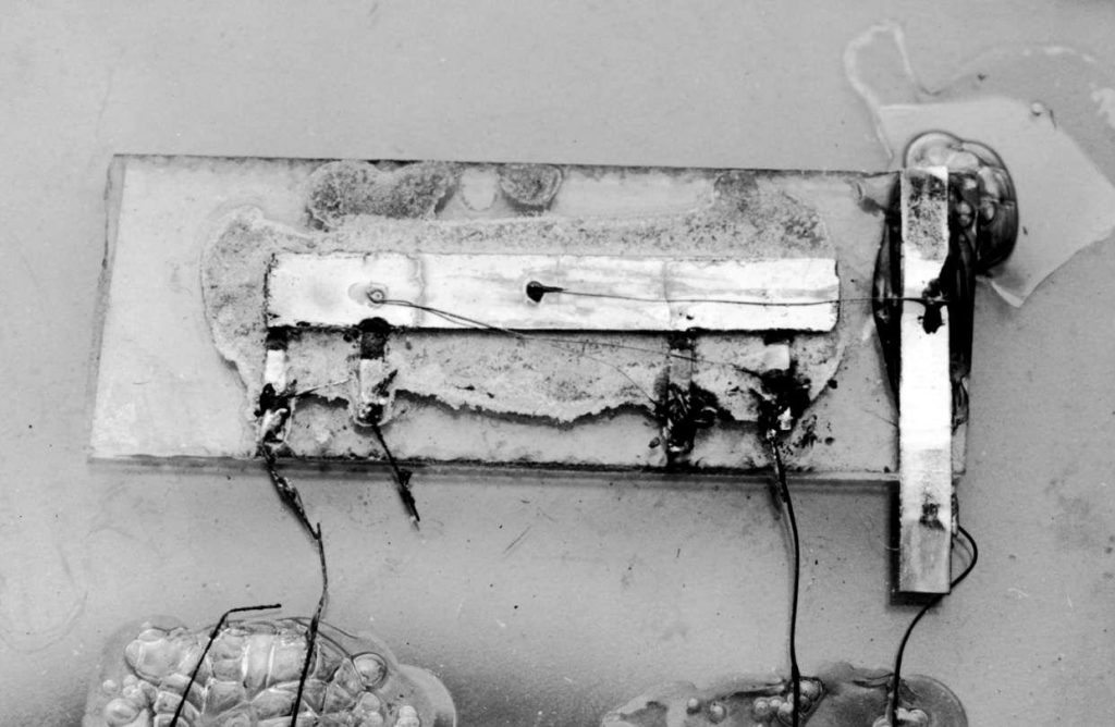
Jack Kilby's “solid circuit” with hand-wired connections. Photo: Texas Instruments
Hall met with Kilby in Dallas in May 1959 to discuss reducing the size of his Polaris system using the new technology. The Navy funded the purchase of 64 units of a custom version of the circuit for Hall's application at $1,000 each for evaluation purposes. The laborious handcrafting process of building Kilby's device and competing internal priorities within TI delayed delivery of the units to MIL/IL until 1962. As they arrived too late to meet the project schedule, Hall upgraded the Polaris circuit with a silicon transistor in place of the older germanium device.
Historians have remarked that NASA's first contract in support of Kennedy's lunar program was surprisingly not for big things that make lots of smoke and flames but for a small computer to guide, in Norman Mailer's words, “a braincase on the tip of a firecracker.” The August 1959 award to MIL/IL was significantly lacking in detail while demanding in schedule; the first functional computer was required to be delivered in July 1964. Hall, who had been promoted to assistant director for the Apollo program, noted, “If we knew then what we learned later or if a complete set of system specifications had been available at the time . . . the designers might have concluded that there was no solution with the technology available in the early 1960s.”²
The lack of specificity in the computer contract reflected the many unknown aspects of the project at that early stage. According to Hall, numerous changes in “schedules, mission plans, and evolving approaches to spacecraft control” drove conflicting demands in the design of the hardware. Recognizing this dilemma, NASA determined that two versions of the computer, called Block I and Block II, should be built. Block II would incorporate changes arising from experience gained in early unmanned flights.
The Apollo guidance, navigation, and control computer (AGC) evolved from an earlier MIT/IL Mars probe study for the Air Force. In 1960 Ramon Alonso and Hal Laning had designed a computer that used transistors to switch the state of a magnetic core in a logic circuit configuration that minimized power consumption. Alonso later led a group of engineers, including logic designers Hugh Blair-Smith and Albert Hoskins, in the design of a series of experimental models of the computer using this core-transistor logic. The first working version of the AGC based on this approach filled six refrigerator-size cabinets in 1962.
Disappointed by the lack of progress with TI's solid-circuits, Hall continued to follow other semiconductor manufacturers' efforts in circuit miniaturization. In July 1959, Robert Noyce, of Fairchild Semiconductor, filed a patent for a “semiconductor device-and-lead structure” that eliminated the most critical manufacturing problem with Kilby's approach - hand-wiring the chip's separate components into a useful circuit. Hall visited Noyce that year. They likely discussed Fairchild's plans, but Hall but did not disclose any details of their meeting.
Noyce's idea took advantage of a new technique invented by Fairchild cofounder, Jean Hoerni, that employed a silicon dioxide protective coating on top of the semiconductor surface. Called the “planar” process, this enhanced transistor reliability and performance and also proved to have significant advantages in enabling high-volume production of all semiconductor products. It remains a fundamental step in manufacturing today's billion transistor chips. Noyce realized that the insulating property of the silicon dioxide would allow the deposition of a conducting metal pattern on top of the chip to interconnect underlying transistors into a complete circuit without manual wiring.
Noyce's patent described a concept; it did not describe how to accomplish it. In September, Jay Last, another cofounder, assembled a team of engineers and physicists, including Isy Haas and Lionel Kattner, to figure out how to turn the idea into a commercial product. Robert (Bob) Norman, head of Fairchild's applications department, designed a simple logic circuit comprising four transistors and five resistors to form a “flip-flop” storage element. Integrating Norman's design onto a single silicon chip posed many challenges. Over the next nine months Last's group experimented with innovative approaches to implementing the device. They tested their first working unit on May 26, 1960.
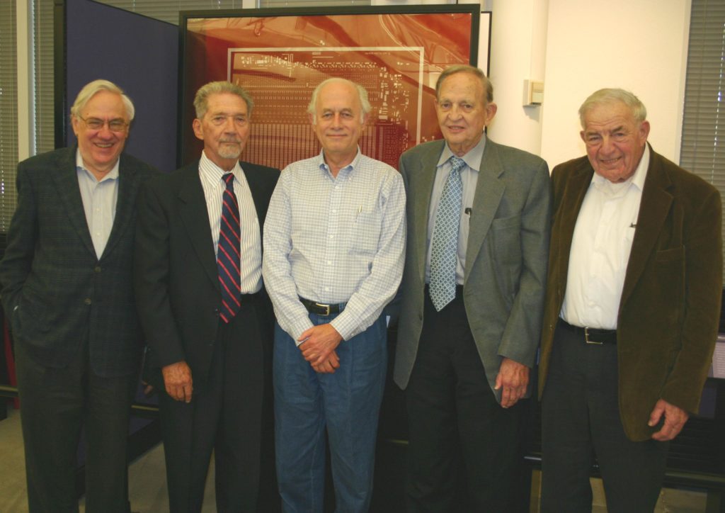
Jay Last, Isy Haas, the author, Lionel Kattner, Bob Norman in 2007. Photo: David A. Laws
This demonstration showed that the concept was sound, but required significant modification to yield a mechanically reliable product. A more robust solution proposed by Haas and Kattner included a 20-hour process in a high-temperature furnace. According to Haas, “the experts said it couldn't be done” without frying the silicon wafers.³ They found a way to overcome the problem and succeed in producing working circuits on September 27, 1960. Fairchild introduced its first commercial IC, a flip-flop element mounted in a round metal can package, under the trade name Micrologic at a New York press conference in March 1961.
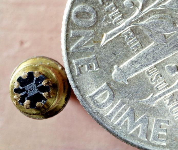
Fairchild's first IC, the “F” element flip-flop compared to a dime coin. Photo: Getty Images
Last's group commenced the design of six additional Micrologic devices to offer a complete family of digital building-block elements for computer designers. Dissension within the company over the allocation of resources to this effort drove Last to quit Fairchild early in 1961, taking Hass and Hoerni with him, to found Amelco Semiconductor. Kattner completed design work on the family, including the “G” element (a 3-input NOR logic gate device), shift registers and adders, before he also departed to found Signetics, the first dedicated IC company, in July.
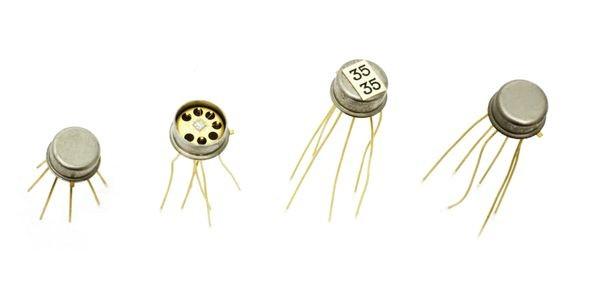
Fairchild “G” Element (3-input NOR gate) IC in metal can package. Photo: © Mark Richards/Computer History Museum
Fairchild introduced the complete Micrologic IC product line in the fall of 1961. Norman became an evangelist for the company, presenting papers at industry conferences and visiting customers to promote the benefits of ICs over discrete transistor solutions. After Norman visited MIT/IL in early 1962, Hall told engineer David Hanley, “Go out and buy large quantities of those things and see if they are real. Then build a computer.” Fairchild delivered an order for 100 devices at $43.50 each in just a few days, convincing Hall of their reality.
After Hanley showed that the computer speed would improve by 2.5 times with a substantial reduction in size and weight, Hall made a presentation to NASA to change the AGC design to ICs. His proposal received approval, and working with engineer Herb Thaler, Hanley completed the prototype machine that occupied four refrigerator size cabinets in early 1963.
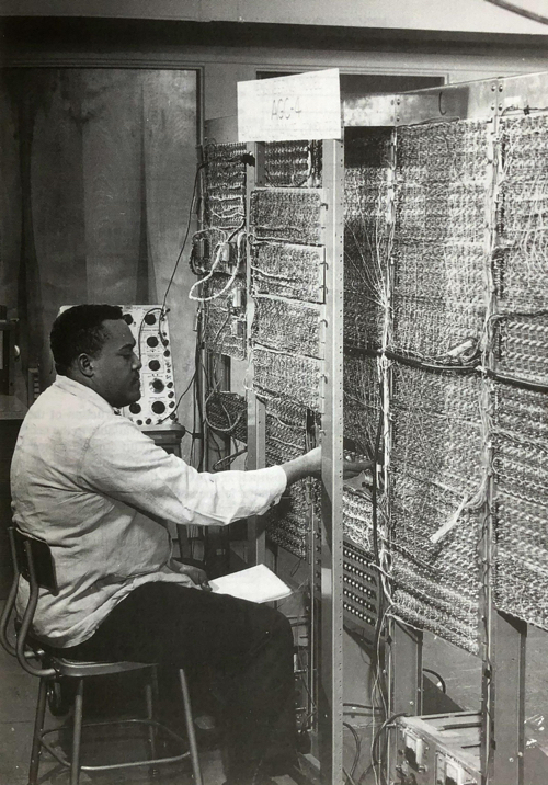
The prototype AGC built by Hanley and Thaler with Fairchild Micrologic integrated circuits. Photo: Charles Stark Draper Laboratory Archives
Competing computer vendors challenged the decision to use ICs due to the lack of proven reliability. Appropriately cautious, but convinced of their potential benefits, NASA required MIT/IL to subject the devices to rigorous testing, analysis, and comprehensive qualification and inspection of their suppliers' manufacturing methods and facilities. Although the Micrologic family comprised a complete set of elements optimized for typical logic functions, Hall elected to build the AGC with a single logic type, the “G” element logic gate, that integrated seven components (three transistors and four resistors) on a chip. His focus on one device type increased confidence in reliability predictions because of the large quantity of units that could be tested.
Hall also contracted with the Norden Division of United Aircraft Corp. to integrate an analog sense amplifier circuit used that used six transistors and eight resistors to detect output signals from the computer's erasable core random access memory and fixed core “rope” read-only memory.⁴ This custom device, one of the first analog ICs, improved precision and reduced the size of 16 sense amplifier modules used in each AGC. To ensure continuity of supply, Fairchild and Signetics also received orders for the analog IC.
Mechanical designers proceeded to squeeze the complex electronic hardware, comprising 4,100 IC packages, magnetic memory elements, and miles of wiring, into the 2 cubic feet allocated in the spacecraft. Memory and IC elements were welded into compact modules that plugged into an outer cabinet fitted with electrical connectors to external systems. The Raytheon Company, a major defense contractor more widely known for inventing the microwave oven, won the contract for production of the ACG in the Waltham, Massachusetts factory. Raytheon's technical director for the Apollo program, Jack Poundstone, managed the complex logistics of transferring the design into the manufacturing facility and the company delivered the first Block I machine to the main contractor, North American Aviation, in August 1964. A Block I computer flew on the first test of the Saturn 1B rocket in August 1966 and later on the unmanned Apollo 4 and 6 missions.
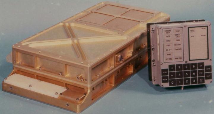
AGC case and keyboard. Photo: NASA
By late 1962, many companies had copied the Fairchild design and developed their own versions of the planar process. Hall placed orders with Motorola, Signetics, Texas Instruments, Transitron, and Westinghouse to qualify additional sources of supply. Only Transitron was able to deliver on time —an indication of the complexity of converting to the new technology.
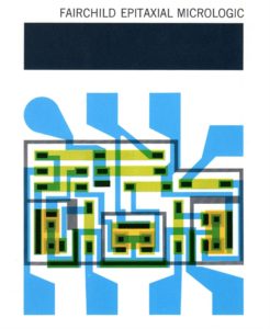
Brochure cover for Epitaxial Micrologic shows an IC mask design drawing (1963). Photo: David A. Laws
During 1963 the project consumed 60 percent of the integrated circuit production in the United States. Even Fairchild was having trouble meeting the demand. Manufacturing yield had been adequate to support modest introduction quantities, but required major improvement to satisfy this rate of growth. The long time, high-temperature process step continued to present problems. James “Phil” Ferguson, who ran the Device Development Section of the R&D Lab, said, “It was very hard on the lattice of the crystal. It was very hard on the oxide and very hard on us.”⁵ Ed Porter, who was earning his engineering degree while working at Fairchild as a technician, suggested that they try a new method of growing special silicon layers on the wafer, called epitaxy, that had recently been developed for transistors. When implemented in production, yields improved by a factor of more than 25 times. The Micrologic drought over, Fairchild shipped the majority of nearly 200,000 circuits procured for Block I systems at an average price of $20–30 each.
Coupled with advances in manufacturing equipment, the epitaxial process also enabled the design of smaller, faster, and lower power circuits. In 1963, under the direction of Bob Norman, Don Farina designed a Milliwatt Micrologic IC family that used one third the power and ran at the same speed as the first generation. Several more complex elements joined the family, including two logic gates on a single chip that could replace two separate first-generation “G” elements. This dual device was available in a flat package that offered twice the logic capability in a smaller area than its predecessor. It became the basic logic element employed in the Block II second generation AGC.
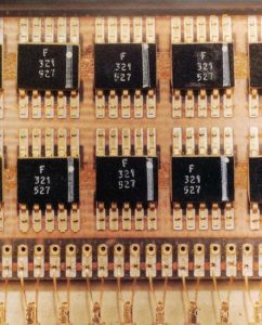
Fairchild Block II flat package ICs on a printed circuit board. Photo: Charles Stark Draper Laboratory Archives
With data gathered from experience with the Block I design, NASA gave the go ahead for development of the planned Block II generation in mid-1963. The availability of more logic in less space offered by the new dual chip “opened the door to a flood of improvements, which the computer designers found difficult to resist.” The end result was a machine that was smaller, faster, and consumed less electrical energy while offering more computing power. MIT/IL completed and released the design to Raytheon for production in July 1965.
Boosted by credibility engendered by the Apollo commitment, dramatic price reductions, and faster, more capable products, the IC business was booming. Burroughs Corporation alone planned to purchase 20 million units of a new IC family from Fairchild for its groundbreaking B2500 series of mainframe computers. Mainstream vendors were short of manufacturing capacity and less interested in devoting scarce resources to the exacting demands of the Apollo project.
The Ford Motor Company purchased Philco, an early leader in transistor manufacturing and one-time employer of Robert Noyce, in 1961. The company saw the Apollo project as an opportunity to re-establish a foothold in the semiconductor business, and in 1964 negotiated a cross-licensing agreement with Fairchild to produce Micrologic. Philco quoted a lower price than other vendors and agreed to establish a dedicated production line in the Lansdale, Pennsylvania factory. Fairchild enjoyed royalties from the business, but Philco-Ford produced the majority of the 800,000 units used in Block II computers that flew in all manned missions, including the first moon landing in 1969.
Two AGCs (one in the Command Module, the other in the Lunar lander) flew in nine lunar and five Earth-orbital missions with zero failures. Confounding critics who advised that integrated circuits were unproven and too risky for such an important project, the computer gained the reputation of being the most reliable piece of electronic equipment on the spacecraft. The Block II version used 2,756 flat pack ICs containing 5,530 logic gates implemented with a total of 16,536 transistors. Because of Hall's decision to use a single IC type to simplify reliability testing, many of the logic gates were not used to their full capacity. The number of active transistors is estimated to be less than half the total available. Data from that period predicts a far higher statistical failure rate for an equivalent discrete transistor version of the AGC than for ICs.
On the night before splashdown on July 23, 1969, Neil Armstrong concluded his final TV broadcast from Apollo 11 with the message:
According to Paul Cerruzi, curator emeritus of the Space History Department at the Smithsonian National Air and Space Museum:
The Apollo program blazed new trails, not only in space exploration but in many areas of science and technology. The AGC project pioneered miniaturized electronics by shrinking a room-sized computer down to a briefcase. It also made a huge leap forward in software development. For the first time, a software program would be used in real time to control actions that could impact the lives of humans. Both of these developments continue to play a significant role in our modern digital world of smart phones and artificial intelligence.