
Non-Volatile Memory (NVM) devices are read/write, electronic data-storage elements that continue to hold information after power is removed from the device. They include magnetic disk-drive units and certain semiconductor chips. Semiconductor NVM devices play important roles in every aspect of the digital universe, from storage cells in vast databanks in the cloud to personal portable devices, and comprise one of the largest segments of the $400-billion semiconductor industry today.
As with every significant semiconductor product development, from the transistor to the microprocessor, NVM devices evolved from the work of pioneering researchers who built on the efforts of their predecessors through intuitive insights, lucky breaks, trial and error, and a determination to ignore the doubts of naysayers. This article is a chronological presentation of some of those pioneers and their key technology developments from the first glimmerings of the idea at Fairchild in 1960 to the high-volume manufacture of Flash chips in the last decade of the 20th century.
The late Jeff Katz and others recorded interviews with a number of significant contributors to advances in the development of commercial semiconductor NVM devices for the Computer History Museum collection of oral histories. Many of the personal comments quoted below are drawn from transcripts of these interviews that may accessed online from hyperlinks in the text.
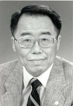
Chih-tang Sah, ca. 1989
C. T. (Tom) Sah at the Fairchild R&D Laboratory, Palo Alto, CA reported in 1961 that charge can be stored “for a long time (several days)” on the gate electrode of an MOS Surface Controlled Tetrode transistor.¹ He noted that in discussions with Fairchild founder and associate research director Victor Grinich and engineer Frank Wanlass, they “recognized immediately its potential as a floating gate memory device.”² They did not pursue the product idea at that time as the company was preoccupied with resolving fundamental start-up stability issues with the MOS process..
The earliest documented descriptions of charge-trapping storage cells emerged from laboratories on both coasts in the mid-1960s. At the Westinghouse Central Research Laboratory, Churchill Borough, PA, in 1966 Edgar A. Sack, Ting L. Chu, and others used a Metal-Nitride-Oxide-Silicon (MNOS) structure as a charge-trapping element.³ Chu and J. R. Szedon described the Westinghouse MNOS element at the 1967 Solid State Device Research Conference in Santa Barbara, CA. The technology was transferred to the Youngwood, PA Semiconductor Division for the design of electronic artillery fuses to replace mechanical fuses.

Boxcar-style clean room at Westinghouse, Semiconductor Division, Youngwood, PA, ca. 1959. Photo: E. A. Sack
Also in 1967, six scientists led by Richard Wegener at the Sperry Rand Research Center, Sudbury, MA described an electrically-alterable, non-destructive read-only MNOS charge-trapping storage device.⁴ In a 1968 report to NASA on “Investigation of New Concepts of Adaptive Devices.” Wegener claimed MNOS as “the first semiconductor device that permits electrically alterable, nonvolatile storage of information.”⁵
Dov Frohman-Bentchkowsky joined the Fairchild R & D laboratory in Palo Alto, CA in 1965. In tandem, he pursued a Ph.D. on “Charge Transport and Trapping in MNOS Structures and its Memory Applications” at U.C. Berkeley “where I knew more about the topic I was dealing with than most of the professors.” (Frohman, Dov — Oral History with Brock). He began the process of applying for a patent based on this work that was submitted after he had left the company. His filing includes the mask design for a 9-bit, word-organized MNOS memory that he fabricated to demonstrate the feasibility of large-scale integrated storage arrays.⁶
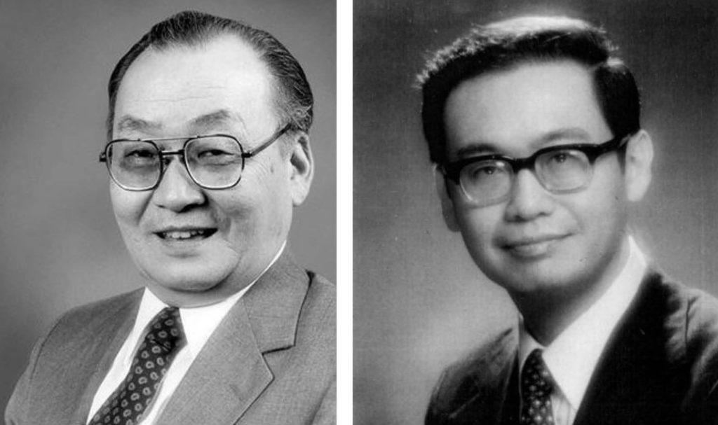
Dawon Khang and Simon Sze
While studying a four-layer cheesecake at lunch at Bell Telephone Laboratories (BTL), Murray Hill, NJ. in 1967, Dawon Khang and Simon Sze came up with the idea of adding a fourth, floating, layer to store charge an MOS transistor. They fabricated a couple of dozen units in the lab to demonstrate feasibility. “About the longest one was one hour, before its electrons were leaking out.” [Sze, Simon — Oral History] According to Sze, “My boss … said, this is absolutely useless. … Can you imagine any reason this would be useful?” They were permitted to publish their results “A floating gate and its Application to Memory Devices,” in the Bell System Technical Journal in July 1967 but BTL did not pursue their idea. “It was just put on the shelf.”
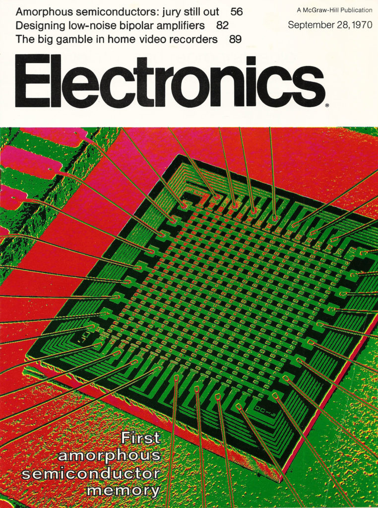
ECD/ Intel 256-bit amorphous semiconductor RMM, 1970
Serial inventor and entrepreneur, Stanford R Ovshinsky created a stir in the scientific community with his 1968 announcement in the New York Times of the Ovonic Memory Switch. Developed at his Energy Conversion Devices (ECD) laboratory in Troy, Michigan, the device employed non-crystalline chalcogenide materials to create a switch that turned on or off when an applied voltage reached a certain magnitude. Ovshinsky claimed that it would yield smaller, faster, simpler, more reliable, and much cheaper electronic circuitry than was possible with transistors. Charles Sie, who worked on the switch at ECD as a graduate student, highlighted a key benefit of the technology as “you could store there forever, (with no limit to the data retention time).” [Sie, Charles — Oral History]
Robert Noyce and Gordon Moore, who had recently co-founded Intel, cooperated with Ovshinsky to explore the technology for a nonvolatile memory to complement their forthcoming bipolar and MOS RAM products. In a 1970 article co-written with Gordon Moore, Ron Neale and D. L. Nelson of ECD describe a 256-bit Read Mostly Memory (RMM) consisting of a film of amorphous semiconductor material between two molybdenum electrodes.⁷ Intel did not pursue the product beyond this demonstration of concept but it was revived as the basis for 3D XPoint phase change memory announced by Intel and Micron in 2015 and productized by Intel under the brand name Optane.
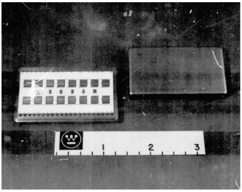
Westinghouse multichip BORAM module, ca. 1975.
MNOS non-volatile memory devices proved attractive to aerospace and defense system designers of the early 1970s. The US Air Force awarded Sperry Rand a contract to develop a 1,024-bit EAROM array and Westinghouse designed electrically-alterable Block-Oriented RAM (BORAM) hybrid modules for the US Army and other customers. Multiple chips mounted on ceramic substrates delivered light weight and compact volume for airborne and portable systems.
Dov Frohman continued to pursue MNOS storage technology after joining Intel in 1969. But while studying stability problems caused by charge migration in the company’s new silicon gate process, he conceived an alternative idea of storing charge on a floating gate conductor. “That was the evolution of what I called then the FAMOS (Floating-gate Avalanche-injection Metal Oxide Semiconductor) device. … the basis of the EPROM.” [Frohman, Dov — Oral History with Katz] He was unaware of the Khang/Sze Bell Labs work until filing for a patent on the architecture.
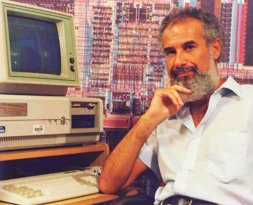
Dov Frohman-Bentchkowsky circa 1971. Photo: Intel Corporation
Frohman ceased further work on MNOS storage to focus his efforts on designing a floating-gate product and Intel introduced his 1702, a 2048-bit EPROM, in 1971. EPROM devices were programmed electrically but could only be erased and reused after physically exposing the chip to UV radiation through a quartz window in the package. Lower-cost, One-Time-Programmable (OTP) versions that did not require the expensive window for erasure proved popular in support of microprocessor-based (MPU) systems. Multiple generations of bigger, faster EPROMs comprised Intel’s most profitable product line until the mid-1980s.
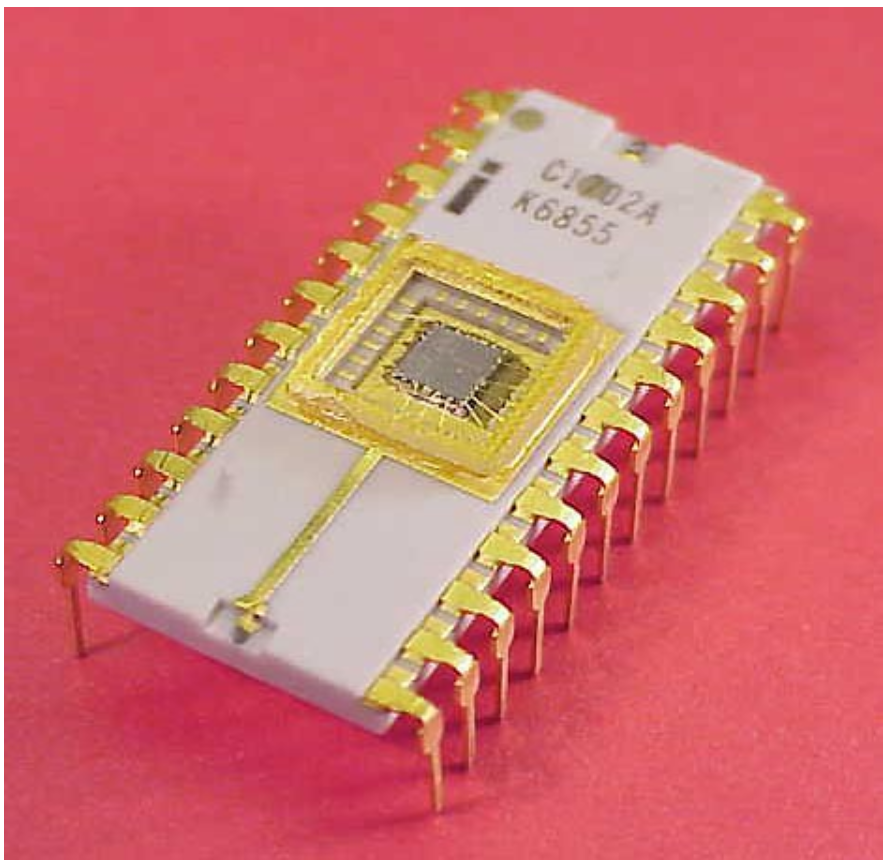
A quartz window admits UV light for EPROM data erasure
Japanese semiconductor manufacturers were quick to recognize the market opportunity for the EPROM. IC pioneer Yasuo Tarui of the Electrotechnical Laboratory in Tokyo and others proposed a floating-gate device at a 1971 Solid State Device conference in Tokyo.⁸ Many research papers and successful commercial products followed from Japanese companies.
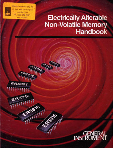
GI EAROM Handbook, 1983
Ed Sack moved from Westinghouse to General Instrument Corporation, Hicksville, NY, in 1969. He served as Vice President and General Manager of the Microelectronics Group that commercialized MNOS technology for consumer electronic applications. His comparison of Westinghouse as a “Gentlemen’s Club with a Side of Politics” to GI as “Lower East Side Manhattan with a Side of Street Brawl” highlights the significant cultural differences between military and commercial semiconductor operations of the era. [Sack, Ed — Personal Account]
GI’s 1975 introduction of the ER1400 Bit-Serial EAROM coupled with the CP1600 16-bit MPU (jointly developed with Honeywell) for a digital, all solid-state TV tuner chip-set resulted in shipments of millions of units. GI continued to produce low-cost EAROM devices for general consumer applications for decades
Other manufacturers who explored MNOS non-volatile memory technology included McDonnell Douglas, Mitsubishi, NCR, and RCA. However, the rapid increase in device density at ever lower cost per bit delivered by intense competition in floating-gate products established the EPROM as the preferred NVM solution for most applications.
Enhancements, such as electrically erasable devices, further entrenched floating-gate as the preferred solution. At Hughes Microelectronics, Newport Beach, CA in 1976, Eli Harari came up with “the idea that if you thin down the gate oxide of the Frohman-Bentchkowsky device from 1,000 angstroms, to 100 angstroms, then that would allow you to program and erase electrically” thus eliminating the need for time-consuming external UV erasure. [Harari, Eli — Oral History] In 1980, Hughes introduced the 3108, a CMOS 8K-bit, Electrically-Erasable PROM (EEPROM) as well as a static RAM chip backed by a nonvolatile cell, called a NOVRAM.

George Perlegos
George Perlegos contributed to several important NVM developments at Intel, including the company’s first EEPROM, the 2816, 16K-bit device in 1978. Together with Gordon Campbell and Phil Salisbury, Perlegos founded SEEQ Technology in 1981 where, to eliminate the need for a separate high-voltage supply in the system, Perlegos led the development of the 5213, a single 5-volt supply EEPROM in 1982. His design incorporated an on-chip charge pump to produce the voltage necessary to support programming. “We had to develop charge pumps small enough that they could go on every column and in every row in order to develop a memory like that.” [Perlegos, George — Oral History] To encourage their use in high-reliability applications, SEEQ also promoted the devices as capable of enduring a minimum of one million write cycles.
Raphael Klein, a former process engineer at National Semiconductor, founded Xicor, Milpitas, CA in 1978 to focus on NOVRAM and EEPROM devices, Xicor shared the early market growth with SEEQ but, unable to compete in high-volume, low-cost applications, the company quit the business in 2001.
In 1980, Fujio Masuoka at the Toshiba, Research and Development Center in Kawasaki, Japan recruited four engineers M. Asano, H. Iwahashi, T. Komuro, and S. Tanaka, to work on an NVM chip.to serve high-volume, low-cost applications. Existing EPROMs used two transistors per memory cell. They designed a smaller, single-transistor cell connected in a manner resembling a NOR logic gate. Masuoka’s colleague Shoji Ariizumi suggested the name “flash” because erasure would happen as quickly as a flash of a camera. Masuoka described the NOR Flash cell at the 1984 International Electron Devices Meeting (IEDM) in San Francisco. Although he succeeded in reducing the cell size, Toshiba did not pursue the invention commercially because of manufacturing issues with the required triple-poly silicon process.
According to Harari, Satyen Mukherjee and Thomas Chang at start-up Exel Microelectronics, Inc. of San Jose, CA designed a flash structure that was manufacturable and became the foundation of what Intel later called NOR flash.
Fujio Masuoka
While assigned to Washington DC to defend the company in patent litigation with TI, Masuoka conceived the idea for a NAND Flash architecture that promised an even smaller cell size and higher write and erase speeds compared to his NOR solution. On his return, Masuoka asked “Mr. Hiseo Tajiri, who was the head of Toshiba consumer electronics development, if the digital camera with four-megabit NAND flash memory would replace film.” [Masuoka, Fujio — Oral History] Tajiri’s realization that NAND could indeed replace film led to the camera division funding the project. Masuoka described the device at the 1987 IEDM in Washington and production of 16-Megabit NAND Flash chips begin in 1992.
Unhappy with what he saw as Toshiba’s failure to reward his work, Masuoka quit in 1994 to become a professor at Tohoku University. Bucking Japan’s culture of company loyalty, he sued his former employer demanding compensation, settling in 2006 for a one-time payment of ¥87m ($758,000).
Stefan Lai joined Intel, Santa Clara, CA to develop a scalable EEPROM technology. Working with Dick Pashley, he devised a means of adding an electrical erase function to the existing smaller EPROM cell to create a NOR Flash architecture that could be fabricated with a standard manufacturing process. As the NVM Division claimed it would not work, they met with Gordon Moore who said “I’ll take care of it. Just sit tight.” [Intel Flash Memory Team — Oral History] Assigned to start a new Flash business unit in Folsom, CA, Pashley and Lai, with designer Niles Kynett, demonstrated working chips in 1986 and a 256K-bit NOR Flash product in 1987.
By the late-1980s, the worldwide market for semiconductor NVM devices of all technologies surpassed two billion dollars. The most popular products of that era comprised 64K, 128K, 256K, and 1 Megabit EPROMs, with the first 2 Megabit units beginning to appear.⁹ US manufacturers, dominated by AMD, Intel, Motorola, SEEQ, and TI, supplied about 50 percent of the world revenue. The remainder was shared between European, predominantly SGS-Thompson, at 10 percent, and Japanese suppliers (Fujitsu, Hitachi, Mitsubishi, NEC, Oki, Toshiba) at 40 percent, although their shipments were limited by government (MITI) imposed production quotas.
The decade of the 1990s saw Flash technology create new system opportunities for NVM devices in both NAND and NOR configurations. NOR Flash architecture has advantages of random access and short read times, and its execute-in-place (XIP) feature makes it ideal for code execution and thus data processing applications. NAND Flash has a slower read speed but a much smaller cell size, permitting higher density devices at lower cost per bit that are ideal for mass storage applications. In addition, NAND’s block read/write access mimics that of disk drives.
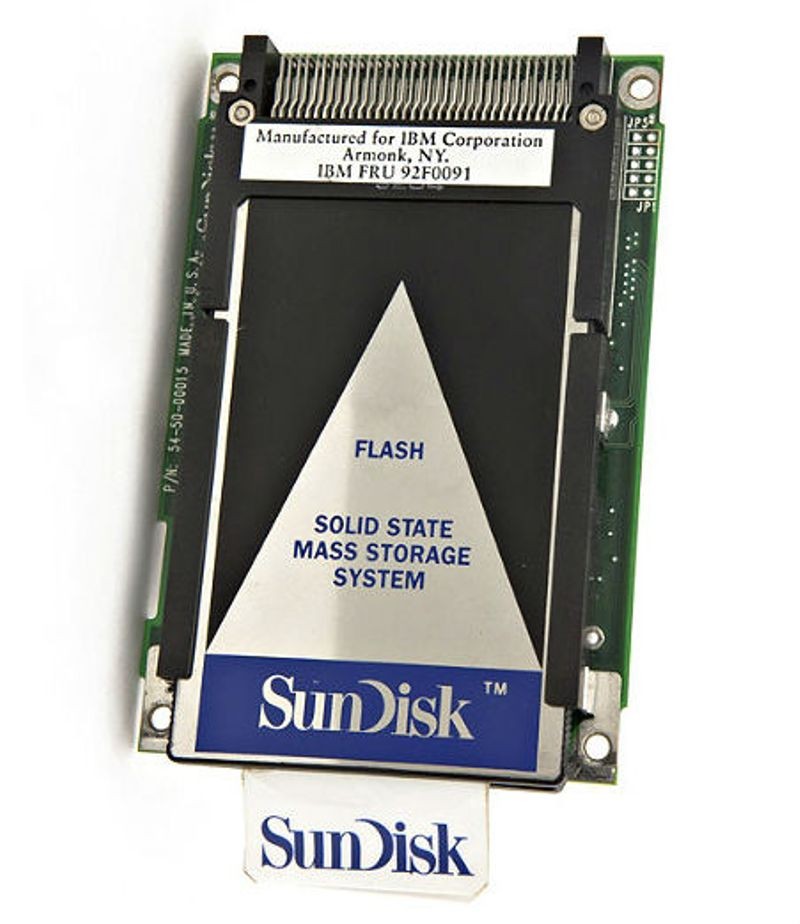
SunDisk (later renamed SanDisk) prototype SSD module for IBM (1991)
Eli Harari, who pioneered thin-oxide processing at Hughes Aircraft in the 1970s, founded SunDisk (now SanDisk) in 1988 to develop mass storage products based on flash memory. He was soon joined by cofounders Jack Yuan and Sanjay Mehrotra and system architect Robert “Bob” Norman. Their first major order was for 10,000 units of a 20-megabyte, 2.5-inch, plug and play compatible ATA, Flash drive to replace a 20-megabyte Connor hard disk in a ThinkPad PC for IBM in 1991. At that time flash reliability was poor, but Harari was encouraged with customer feedback on the prototype units: “If I can run several units over the weekend, with no failure, then you have a good product.” [Harari, Eli — Oral History]
It took several generations of Flash process and system design improvements to achieve the levels of reliability demanded by commercial applications. Harari’s incorporation of embedded metadata allowing for error correction to be managed by firmware, thus masking early reliability issues from the user, was a critical factor in the acceptance of the technology. High-volume notebooks using SSDs entered the market in the late 2000s, and today SSDs comprise the fastest growing segment of the computer storage market.
SanDisk Founders Yuan. Mehrotra, and Harari
New opportunities opened for SanDisk after the company introduced Compact Flash cards for digital cameras in 1994. According to Mehrotra “instead of somebody else selling the film, or the camera manufacturers sel ling the film, we realized that there was a large aftermarket for flash cards. So, taking flash cards into the aftermarket, … making it a global brand, was a transformative piece of the company’s history.” [Mehotra, Sanjay — Oral History] Western Digital acquired SanDisk in 2016.
Today Flash technologies dominate the market for NVM devices that in 2019 exceeded $50-billion and comprised the largest product segment of the worldwide semiconductor industry. Samsung has emerged as the world’s largest supplier of Flash chips with around 30 percent of the market. Other major vendors include Toshiba and Western Digital.
Each year the Flash Memory Summit recognizes individuals who have shown leadership in promoting the development and use of Flash memory and related technologies with a Lifetime Achievement Award (LAA). Awardees who have not been mentioned above are Kinam Kim of Samsung for his advancements in 3D NAND and Dov Moran and Aryeh Mergi of M-Systems for innovations including embedded flash for cell phones, flash file systems, and the USB flash drive.