
On reading my recent @CHM blog “Who invented the diode?” CHM senior curator Dag Spicer pointed me to a fascinating scholarly treatise, “Singletons and Multiples in Scientific Discovery: A Chapter in the Sociology of Science,” that describes how multiple independent discoveries of scientific phenomena are the norm rather than the exception. The author, Robert K. Merton, traces this understanding back to Elizabethan philosopher, statesman, and scientist Sir Francis Bacon.
Merton also paraphrases Bacon’s observation that “once the right path is followed, discoveries in limitless number will arise from the growing stock of knowledge.” This pattern was readily apparent in the history of the diode. And as this blog describes, it was repeated in the development of the next great leap forward in semiconductor devices, the transistor.
Early in the last century scientists knew how to make a two terminal diode by placing a sharp metal probe in contact with a semiconductor crystal. These point-contact diodes could change an oscillating signal to a steady signal and found wide use as detectors in crystal radio receivers. By the 1920’s inventors began to investigate the use of semiconductors for amplifying and switching signals.
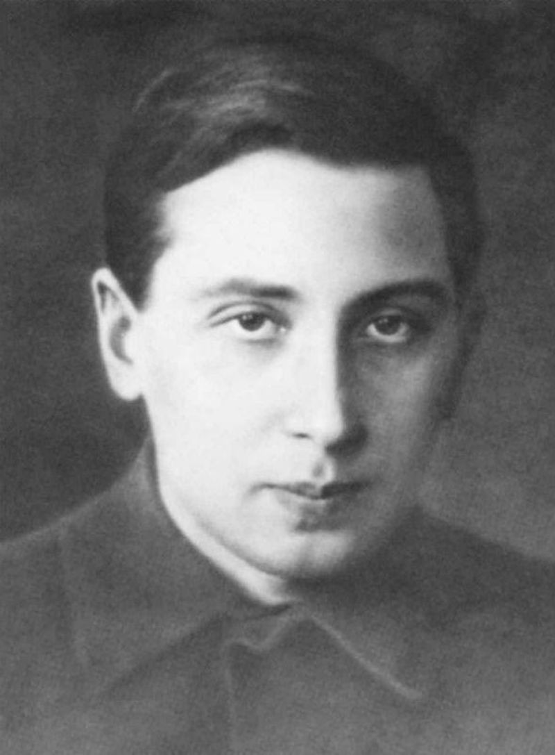
Oleg V. Losev (1903 – 1942)
Some of the earliest work on semiconductor amplifiers emerged from Eastern Europe. In 1922-23 Russian engineer Oleg Losev of the Nizhegorod Radio Laboratory, Leningrad, found that a special mode of operation in a point-contact zincite (ZnO) crystal diode supported signal amplification up to 5 MHz. Although Losev experimented with the material in radio circuits for years, he died in the 1942 Siege of Leningrad and was unable to advocate for his place in history. His work is largely unknown.
Austro-Hungarian physicist, Julius E. Lilienfeld, moved to the US and in 1926 filed a patent for a “Method and Apparatus for Controlling Electric Currents” in which he described a three-electrode amplifying device using copper-sulfide semiconductor material. Lilienfeld is credited with inventing the electrolytic capacitor but there is no evidence that he built a working amplifier. His patent, however, had sufficient resemblance to the later field effect transistor to deny future patent applications for that structure.
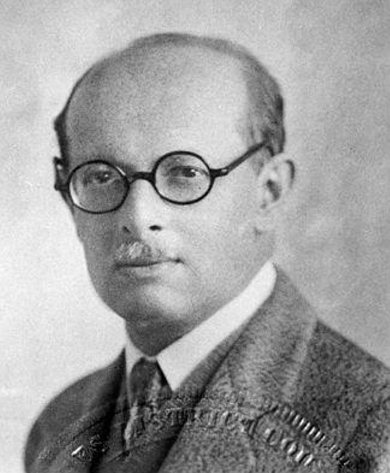
Julius E. Lilienfeld (1882 –1963), Courtesy of AIP Emilio Segre Visual Archives
German scientists also contributed to this early research. While working at Cambridge University, England in 1934, German electrical engineer and inventor Oskar Heil filed a patent on controlling current flow in a semiconductor via capacitive coupling at an electrode – essentially a field-effect transistor. And in 1938, Robert Pohl and Rudolf Hilsch experimented on potassium-bromide crystals with three electrodes at Gottingen University. They reported amplification of low-frequency (about 1 Hz) signals. None of this research led to any applications but Heil is remembered in audiophile circles today for his air motion transformer used in high fidelity speakers.
Because of their poor reliability and large power consumption, by the late 1930’s engineers at American Telephone and Telegraph knew that vacuum-tube circuits would not meet the company’s rapidly growing demand for increased phone call capacity. Bell Laboratories’ director of research Mervin J. Kelly assigned William Shockley to investigate the possibility of using semiconductor technology to replace tubes.
Using improved semiconductor materials developed for radar detectors during the war, in early 1945 Shockley experimented with a field-effect amplifier, similar in concept to those patented by Heil and Lilienfeld, but it failed to work as he intended. Physicist John Bardeen suggested that electrons on the semiconductor surface might be blocking penetration of electric fields into the material. Under Shockley’s direction, together with physicist Walter Brattain, Bardeen began researching the behavior of these “surface states.”
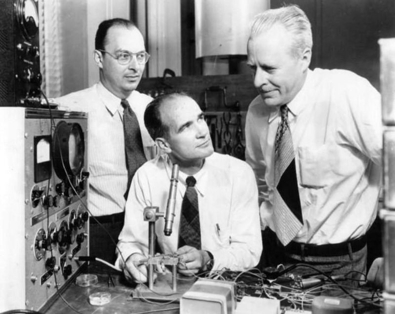
John Bardeen, William Shockley and Walter Brattain in 1948, Courtesy of Bell Telephone Laboratories
On December 16, 1947, their research culminated in a successful semiconductor amplifier. Bardeen and Brattain applied two closely-spaced gold contacts held in place by a plastic wedge to the surface of a small slab of high-purity germanium. On December 23 they demonstrated their device to lab officials and in June 1948, Bell Labs publicly announced the revolutionary solid-state device they called a “transistor.”
Early that same year, while examining a phenomenon he called “interference,” German physicist Herbert Mataré and his colleague Heinrich Welker independently fabricated an amplifier based on germanium with two point-contacts touching its surface at a Westinghouse laboratory in Paris, France. When they learned of the Bell Labs’ announcement, Mataré and Welker applied for patents on their own device, which they called a “transistron.”
Realizing that the point-contact structure had serious limitations, and spurred by professional jealousy as he resented not being involved with its discovery, Shockley worked alone to conceive a more reliable and reproducible device. Introduced in 1952, Shockley’s bipolar junction transistor, which was made from a solid piece of semiconductor material and no point contacts, dominated the industry for the next 30 years. All three Bell Labs scientists received the 1956 Nobel Prize in Physics for their contributions.
Over the next decade many different manufacturing methods were developed to produce faster, cheaper and ever more reliable transistors. An important advance in 1954 was the silicon transistor, first from Morris Tanenbaum at Bell Labs and shortly after by a team led by chemist Willis Adcock at upstart Texas Instruments. By the end of the 1950s, silicon had become the industry’s preferred material and TI the dominant semiconductor vendor.
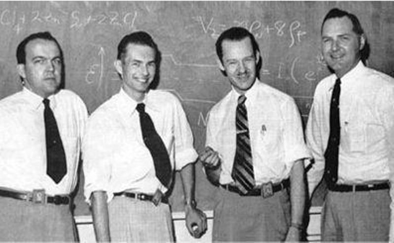
The 1954 Texas Instruments’ silicon-transistor team: W. Adcock, M. Jones, E. Jackson, and J. Thornhill, Courtesy of Texas Instruments, Inc.
The founders of Fairchild Semiconductor, a start-up in California’s Silicon Valley, started their company on the premise of making an even better silicon transistor. Their day-to-day challenges in developing a new technology are described in detail in several of the Fairchild Patent Notebooks in the Museum collection, notably those written by Gordon Moore and Sheldon Roberts. Coinciding with the beginning of the “space race,” their 1958 introduction of a double-diffused silicon mesa transistor was a great commercial success. Reliability problems that threatened the future of the company were resolved with Swiss physicist Jean Hoerni’s revolutionary planar process. Hoerni’s planar technique not only transformed transistor manufacturing from a semi-hand-crafted operation to high volume automated production. It also enabled the development of the modern integrated circuit (IC).
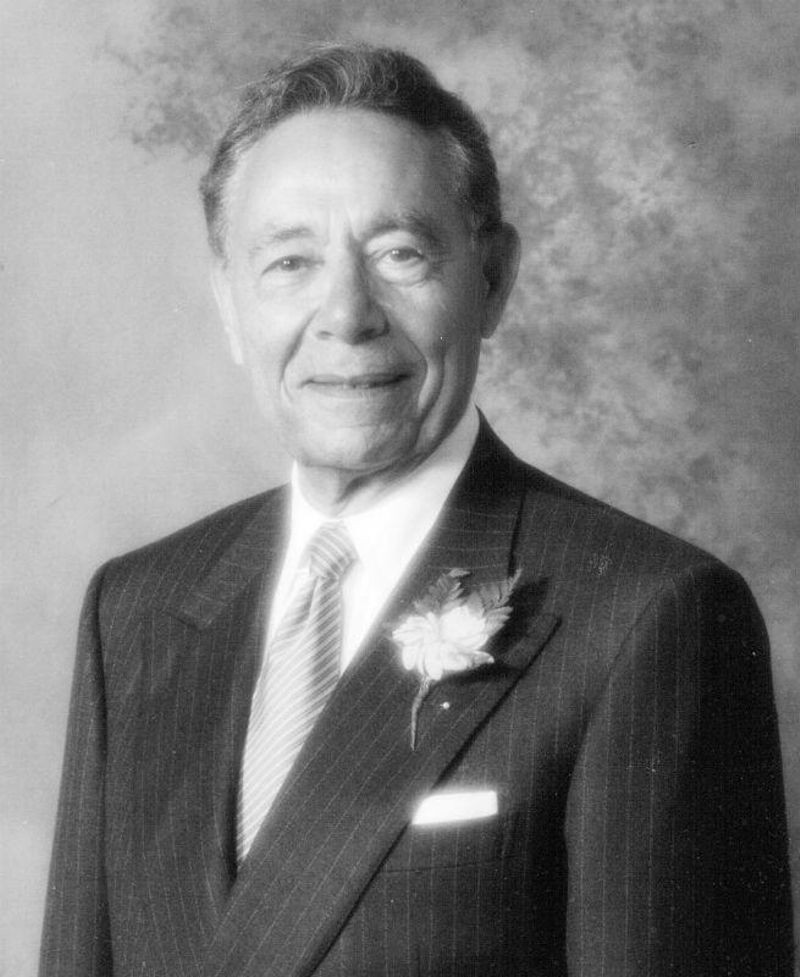
Martin M. Atalla (1924 – 2009), Courtesy of the Atalla Family
The ideas of Lilienfeld and Heil and Shockley’s failed early experiments finally bore fruit in 1959 when, working for Egyptian engineer Martin M. (John) Atalla on the study of semiconductor surfaces at Bell Labs, Korean electrical engineer Dawon Kahng built the first successful field-effect transistor (FET) comprising a sandwich of layers of metal (M – gate), oxide (O – insulation), and silicon (S – semiconductor). The MOSFET, popularly shortened to MOS, promised a significantly smaller, cheaper, and lower power transistor.
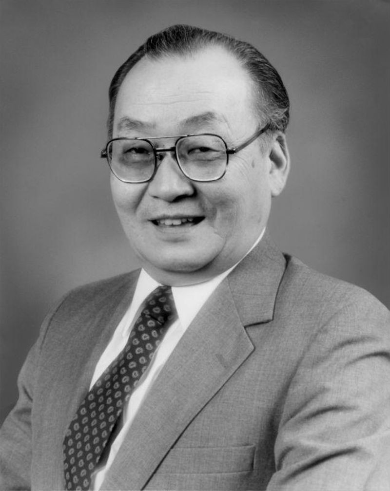
Dawon Kahng (1931 – 1992), Courtesy NEC Corporation
Fairchild and RCA introduced commercial MOS transistors in 1964. But in the decade that it took to resolve early manufacturing problems with the MOS process, individual transistors had largely been replaced by ICs in computer systems. In the long term, MOS transistors proved the most practical approach to building high-density ICs, such as microprocessors and memories. Close to 100% of the billions of transistors manufactured every day are MOS devices.
As with most technological developments, the creation of the modern transistor followed the Baconian pattern of gradually emerging from “the growing stock of knowledge” built by a truly international cast of engineers and scientists rather than from the lone efforts of a single heroic “inventor.”