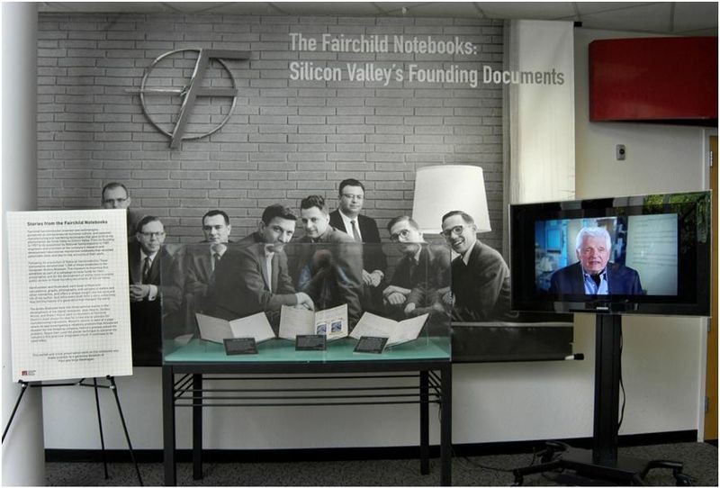

View of The Fairchild Notebooks exhibit in the lobby of the Computer History Museum, May, 2013
The Fairchild Notebooks: Silicon Valley’s Founding Documents, a temporary exhibit in the lobby of the Computer History Museum, displays three iconic volumes from the collection of Fairchild Semiconductor documents donated to the museum by Texas Instruments in 2012. Hand written and illustrated by three of the founders of Fairchild (Jean Hoerni, Gordon Moore and Robert Noyce), each book reveals the story and personality of the author and his work. Collectively they tell the history of the early days of a company and an invention that changed the world.
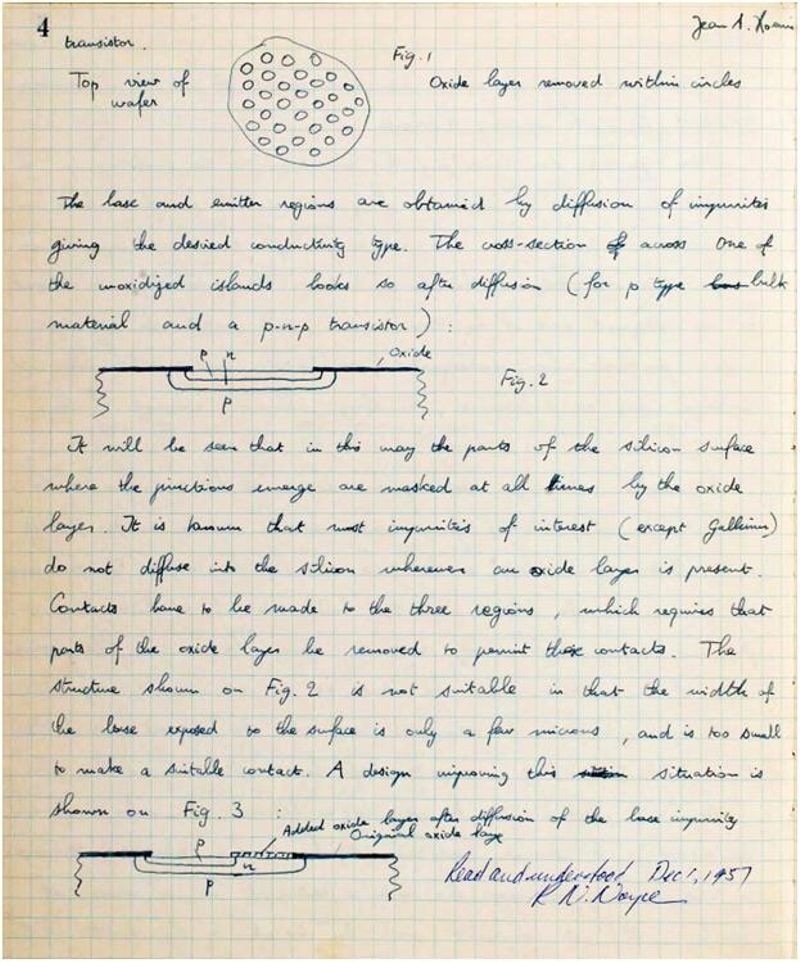
These books were selected for the initial public exhibit of works from the collection to reconstruct the story of how one of the most important early developments in semiconductor technology unfolded. For example, Hoerni’s book is open at a page describing his idea for a new planar process for manufacturing transistors. Moore’s volume is open at a page where he was investigating a reliability problem that threatened disaster for the fledgling company. (Hoerni’s planar process solved the problem and allowed Fairchild to resume manufacturing transistors and stay in business). Noyce’s book shows his original conception of using the planar technique to design the industry’s first practical integrated circuits. This succession of problems and solutions revolutionized the technology and manufacturing of microelectronics and drove the explosive growth of the region we now know as Silicon Valley.
This patent notebook, designated Hoerni (#3), covers the period from late 1957 to December, 1960 shortly before the author left Fairchild to co-found Amelco Semiconductor. A brief biography of the author and summary of his work is posted on the Museum’s Fairchild Notebooks website. An electronic copy of the complete notebook is also available.

Second page of Hoerni’s 1957 disclosure of his planar idea. Witnessed by R.N. Noyce.
On December 1, 1957, just two months after the founding of Fairchild, Hoerni wrote his first expression of the planar process on pages 3-4. “Method of protecting exposed p-n junctions at the surface of silicon transistors by oxide masking techniques,” and describes how to manufacture a transistor by etching tiny windows in a glass layer deposited on the surface of a silicon wafer and leaving it in place to protect the underlying semiconductor junction. The idea lay dormant for more than year while the start-up company focused on immediate issues of survival as it struggled to perfect its first transistors.
The book also contains notes on experimental runs of wafers together with process and design ideas that were used as the basis for important patent filings. Interesting entries include Hoerni’s disclosures on a gold-doping technique for enhancing the speed of silicon transistors that allowed them to compete with germanium devices for applications in high-speed computers, including the groundbreaking Control Data Corporation CDC 6600 supercomputer. In March, 1960, he noted that newly developed epitaxial silicon film technology could render much of Fairchild’s work to date obsolete. This concern proved unfounded as epitaxy was later adapted to improve the yield of planar devices.
This notebook, designated Moore (#6), is one of five by the author in the collection. A brief biography of the author and summary of his work is posted on the Museum’s Fairchild Notebooks website. An electronic copy of the complete notebook is also available.
The volume covers the early period from start-up in October, 1957 to May, 1963 when Moore was R & D director for the company. He maintained an almost day-by-day account of the challenges and issues associated with developing the first double-diffused silicon mesa transistors. Topics include “Noyce suggestion for a pnip structure,” “Built a sputterer.” “First transistors mounted,” and “Return of ‘mistreated’ IBM transistors.” The contents of the volume are perhaps best summarized by his comment on page 66 that “It became apparent that life is not simple.”

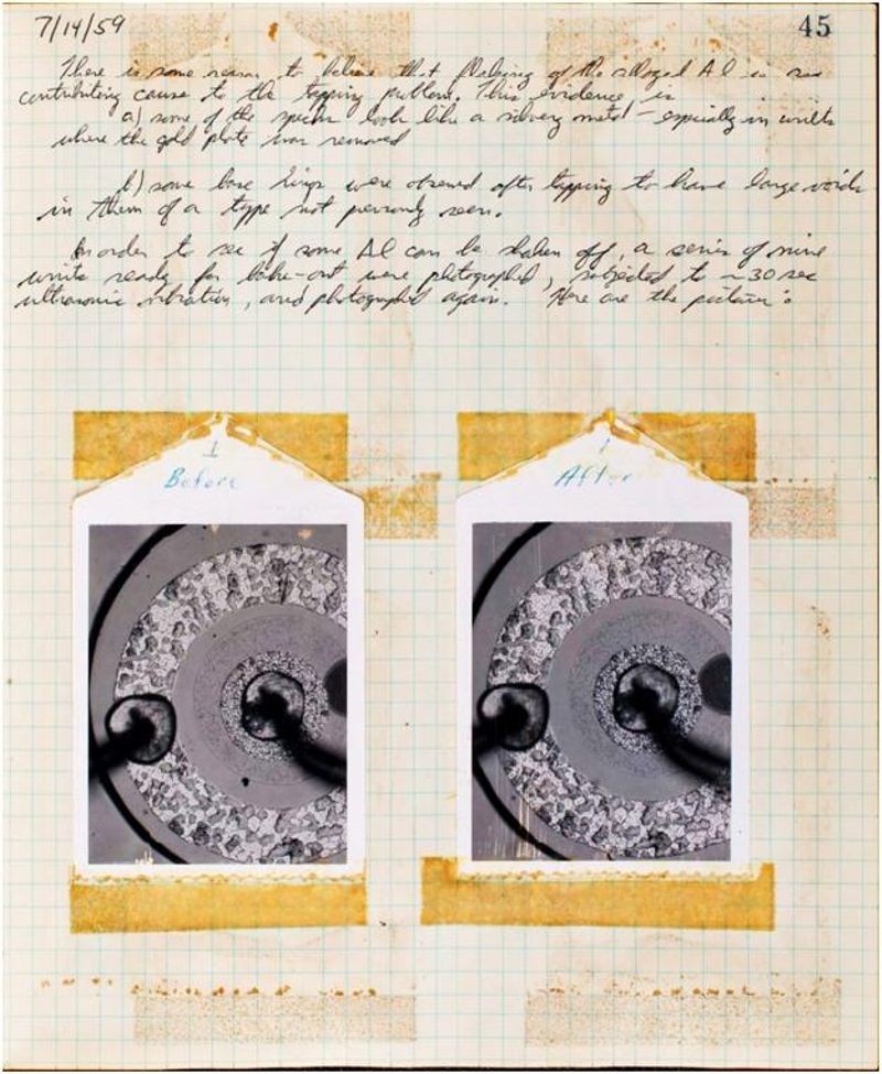
Moore’s Notebook page showing a transistor surface before and after testing for flaking.
In early 1959, Fairchild’s major source of revenue came from supplying silicon transistors to Autonetics for a computer on the USAF Minuteman missile. Reliable operation was of paramount importance. When the customer reported that some devices were failing in the system, shipments were placed on hold until Fairchild resolved the problem. In July, Moore began a series of experiments to diagnose the cause of the failures. He found that when tapping the outer metal package of the transistor, about ten percent of the devices failed. On opening the units, flakes of “silvery metal, possibly Al” and “translucent crud” were found to be shorting-out the exposed mesa junctions. In the exhibit, the notebook is open at pages 44-45. These describe some of the tap test results together with microphotographs seeking the source of the metal flakes. In order to resume shipments to Autonetics, for the next several months every device was mounted in a test circuit and pounded with a hammer to identify bad units before shipment. The long term solution was to use the oxide layer of Hoerni’s planar process to electrically insulate the junction from errant metal flakes.
An interesting side note to this story is that before historians had access to these notebooks, the chronology published in many histories of Fairchild claimed that Hoerni had resurrected the planar process idea he had written in his book in December 1957 specifically in response to this reliability problem. The dated entries in Moore’s book document that the cause of the problem was not identified until July 1959. This is at least 6 months after Hoerni sent a formal disclosure to the company patent attorney and began in earnest to develop and demonstrate the planar process. A question the books do not answer therefore is “What did stimulate his revival of the idea?”
This volume, designated Noyce (#8), covers the period February, 1958 to June, 1966. A brief biography of the author and summary of his work is posted on the Museum’s Fairchild Notebooks website. An electronic copy of the complete notebook is also available.
Noyce’s entries document the extraordinary breadth of his creativity both during his initial service as R&D director and later as vice president and general manager of the company. Numerous invention disclosures in his book include parametric amplifier diodes, optical scanning devices and adaptive machines.

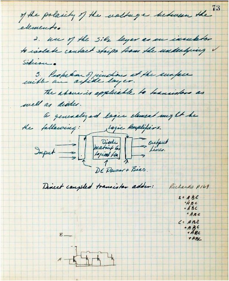
Noyce notebook showing his implementation of an integrated adder function
In the lobby exhibit, the notebook is open at pages 70-71. An entry dated January 23, 1959, titled “Methods of isolating multiple devices,” is the first written expression of his most significant technical contribution to the industry. Noyce states that “In many applications now it would be desirable to make multiple devices on a single piece of silicon in order to be able to make interconnections between devices as part of the manufacturing process and thus reduce size, weight, etc, as well as cost per active device element”. This describes his idea that the oxide layer of Hoerni’s planar process could be used as an insulator to permit the addition of metal traces on the top surface of the wafer and thereby interconnect multiple transistors into an integrated electronic circuit. On page 73, he sketched the structure of a generalized logic element and the circuit implementation of a direct-coupled transistor adder. In July, 1959, Noyce filed an application for a “Semiconductor device-and-lead structure,” his seminal patent based on this idea—the modern integrated circuit.
The combination of Hoerni’s planar process and Noyce’s integrated circuit concept described in this blog is the foundation of the modern semiconductor industry, a $300 billion a year economic powerhouse whose products have transformed human life. Many other such stories are awaiting discovery in the more than 1,000 volumes that comprise the Fairchild Collection. Information on approximately 200 of them and their authors can be accessed on the Museum’s Fairchild Semiconductor Notebooks website.